Introduction
How does a CPU communicate with an NVMe drive, a network card, or a GPU? Most software engineers rely on drivers and kernel modules without thinking about the underlying mechanisms. But when you’re debugging performance issues, tuning interrupt handling, or trying to understand why perf shows certain bottlenecks, you need to know what’s happening at the hardware level.
x86 systems use three primary mechanisms for CPU-peripheral communication:
- Port-mapped I/O (PMIO): The CPU uses dedicated I/O instructions to access a separate address space
- Memory-mapped I/O (MMIO): Peripherals expose their control registers as memory addresses
- Direct Memory Access (DMA): Peripherals transfer data directly to/from RAM without CPU intervention
Modern PCIe devices—your NVMe drives, network cards, GPUs—almost exclusively use MMIO and DMA. PMIO is legacy, primarily seen in older ISA devices and backward compatibility modes. Understanding these mechanisms helps you interpret system behavior: why DMA buffer sizes affect throughput, why interrupt moderation matters for latency, and what kernel parameters like irqaffinity actually control.
This breakdown covers how each mechanism works, their performance characteristics, and where you’ll encounter them in real systems.
Understanding x86 Communication Channels
Modern x86 systems use three primary communication mechanisms to move data between components.
CPU-Memory Bus
The CPU-Memory bus is a dedicated connection between the processor and RAM. Modern CPUs have integrated memory controllers with multiple channels (typically 2-8 depending on the platform). A dual-channel DDR4-3200 configuration provides 51.2 GB/s of theoretical bandwidth to the CPU. No other devices share this bus.
PCIe: Point-to-Point Serial Interface
PCIe (Peripheral Component Interconnect Express) is the lifeblood of modern x86 systems. It serves as the primary conduit through which GPUs, NVMe SSDs, and network cards exchange data. To truly understand PCIe, one must first grasp how it differs from the legacy ‘Bus’ architecture and the critical role of the ‘Root Complex.’
Shared Bus vs. Point-to-Point
Older standards like PCI or ISA were literal ‘Buses.’ Much like passengers waiting at a stop for a single vehicle, all devices shared a single communication line.
- Shared Bus (Legacy): Only one device could transmit data at a time. If a sound card was sending data, the network card had to wait its turn. As more devices were added, contention increased and overall speed plummeted.
- Point-to-Point (PCIe): Each device has a dedicated high-speed lane connected 1:1 to the CPU. Traffic in an adjacent lane (another slot) does not affect your speed. This allows each device to fully occupy its allocated bandwidth and perform Full-duplex communication, where sending and receiving happen simultaneously.
The System Gateway: Root Complex
Since PCIe devices have dedicated roads, they require a ‘Central Terminal’ where all those roads converge. This is the Root Complex.
- Role: It is the massive gateway connecting the CPU and system memory to the PCIe Fabric. Located inside the CPU, it acts as a ‘Traffic Control Center,’ processing all PCIe requests and deciding whether to route data to memory or to another device.
- Top of the Hierarchy: Every PCIe device hangs from a tree-like hierarchical structure with the Root Complex at its base. When we say a “GPU is directly connected to the CPU,” we specifically mean the GPU is using a PCIe port directly wired to the Root Complex to minimize latency.
Specifications
PCIe Lanes: A PCIe connection consists of lanes (x1, x4, x8, x16). Each lane contains two differential pairs—four wires total—one pair for transmit, one for receive. More lanes provide proportionally higher bandwidth:
- x1: One lane
- x4: Four lanes (4× the bandwidth)
- x16: Sixteen lanes (16× the bandwidth)
GPUs typically use x16, NVMe SSDs use x4. An x4 card can fit in an x16 slot.
PCIe Generations
Each generation roughly doubles bandwidth per lane:
- PCIe 3.0: ~1 GB/s per lane (x4 = ~4 GB/s, x16 = ~16 GB/s)
- PCIe 4.0: ~2 GB/s per lane (x4 = ~8 GB/s, x16 = ~32 GB/s)
- PCIe 5.0: ~4 GB/s per lane (x4 = ~16 GB/s, x16 = ~64 GB/s)
These are practical throughput numbers accounting for 128b/130b encoding overhead (~1.5% reduction from raw bit rate). A PCIe 4.0 x4 NVMe SSD can hit 8 GB/s, while PCIe 3.0 x4 maxes at 4 GB/s.
DMA: Direct Memory Access
DMA allows devices to read and write RAM without CPU involvement. Instead of the CPU copying data byte-by-byte, devices access memory directly.
The process:
- CPU tells the device: “Write 64KB to memory address 0x12345000”
- Device uses its PCIe connection to write directly to physical memory
- Device signals completion via interrupt
- CPU processes the result
The CPU only issues commands and handles completion—it doesn’t transfer data. For high-throughput devices like 100GbE network cards or NVMe SSDs moving gigabytes per second, this is essential. Without DMA, the CPU would become the bottleneck copying every packet or disk block.
Going a step further, P2P (Peer-to-Peer) DMA is theoretically possible, allowing devices to communicate directly without even passing through RAM. Typical scenarios include reading data from an NVMe SSD and sending it straight to a GPU, or GPU 0 writing data directly into the VRAM of GPU 1. In reality, however, data frequently detours through the system memory (RAM) for the following reasons:
- Root Complex Boundaries: If data must move between different Root Complexes (e.g., between CPU A and CPU B in a NUMA server), the hardware architecture may forces a path through RAM. Even within a single CPU, multiple Root Complexes may exist.
- OS Policies: Operating systems prefer data to pass through RAM for efficient resource management. Keeping data read from an SSD in RAM allows for much faster subsequent access via the Page Cache and simplifies integrity checks for data tampering. If devices communicate “behind its back,” the OS loses visibility into the system’s data flow. Windows often blocks direct communication between devices via ACS (Access Control Services), viewing it as a security threat. Linux also employs mechanisms like IOMMU or SWIOTLB (Bounce Buffers) for system integrity; before a device can access memory directly, the data is first pulled into a secure area of RAM for validation. However, in Linux, optimization libraries like NCCL (NVIDIA Collective Communications Library) can overcome these constraints. NCCL precisely maps the system topology and, if the hardware supports it, forcibly activates P2P paths between GPUs even when security restrictions are present. Even without such libraries, the Linux kernel’s native I/O design and processing are inherently optimized for high-performance computing.
The real danger of this “U-turn” is Memory Bandwidth Contention. When data is forced to detour through RAM instead of taking a shortcut—whether it’s SSD → RAM → GPU or GPU → RAM → GPU—it occupies the system memory bandwidth twice. As the CPU’s own operations and the devices’ detour traffic fight over the limited DDR memory bandwidth, the overall system throughput eventually decreases.
With these communication mechanisms established, we can now examine the two main ways devices connect via PCIe.
Direct vs Detour: PCIe Connection Methods
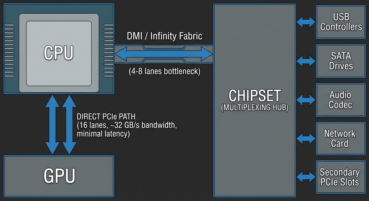
CPU-Direct Connections
Your CPU has 16-20 PCIe lanes (on mainstream platforms) wired directly to the socket. On Intel, these come from the CPU die; on AMD Ryzen, they originate from the I/O die rather than the compute chiplets. HEDT and workstation platforms offer significantly more—Threadripper and EPYC provide 48-128 direct lanes.
CPU-direct connections deliver full bandwidth with no contention. A PCIe 4.0 x16 connection provides ~31.5 GB/s per direction (full-duplex capable, though most workloads don’t achieve simultaneous bidirectional saturation). The primary GPU occupies the first PCIe x16 slot for this reason—exclusive access to direct lanes. On higher-end motherboards, secondary x16 slots may also be CPU-direct. Through PCIe bifurcation, you can split a single x16 connection into x8/x8 for two devices, though each gets half the bandwidth. For dual GPUs, x8/x8 typically causes minimal performance loss (0-5% in most workloads) since GPU workloads rarely saturate PCIe bandwidth.
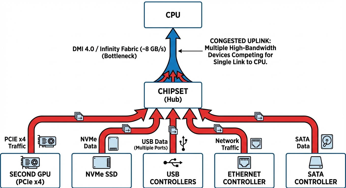
The Chipset: Multiplexing Hub
The chipset aggregates dozens of I/O devices: USB controllers (often 10+ ports), SATA drives, audio codecs, network interfaces, secondary PCIe slots, and legacy I/O.
The chipset communicates with the CPU via a dedicated link. Intel’s DMI 3.0 provides ~4 GB/s (similar bandwidth to PCIe 3.0 x4, though with chipset-specific protocol optimizations); DMI 4.0 doubles this to ~8 GB/s. AMD’s chipset connection varies by platform but typically uses PCIe 4.0 x4 on X570/B550, providing ~8 GB/s.
Everything connected to the chipset shares this link.
Why This Architecture Exists
Manufacturing cost scales with I/O complexity. Each PCIe lane requires SerDes (serializer/deserializer) logic, PHY layers, physical traces on the CPU package and motherboard, and additional pin count. More lanes mean larger die area and lower yields. A CPU with 100 direct PCIe lanes would be prohibitively expensive and require massive motherboards.
Most I/O devices aren’t simultaneously active at full bandwidth. A 1Gbps network card at full utilization uses ~125 MB/s. A USB 3.2 Gen 2 device maxes at ~1.2 GB/s. A SATA SSD peaks at ~600 MB/s. These rarely saturate simultaneously. The chipset exploits statistical multiplexing—aggregating many devices that rarely all need bandwidth at once. Typical chipset utilization hovers around 10-30% even in active workloads.
When chipset bandwidth is exceeded—copying files between NVMe drives connected to chipset M.2 slots (typically the second and third M.2 slots on consumer boards; the first is usually CPU-direct) while streaming video and downloading—devices compete for bandwidth and throughput drops proportionally. The DMI link becomes the bottleneck, and you’ll see transfer speeds crater.
When this matters: You’ll saturate chipset bandwidth when running multiple high-throughput workloads simultaneously: RAID arrays on chipset NVMe slots, 10GbE transfers while copying between SATA drives, or heavy USB 3.2 device usage during storage operations. Single-threaded workflows—gaming, browsing, even video editing with one fast drive—rarely approach chipset limits. If you’re frequently running iostat and seeing aggregate throughput above 7 GB/s across chipset devices, you’re hitting the ceiling.
Devices requiring guaranteed high bandwidth get direct CPU lanes. Everything else shares the chipset link, which works until aggregate demand exceeds capacity.
This dual-path architecture has evolved significantly over time, shaped by competition between Intel and AMD.
A Tale of Two Architectures: Intel vs AMD’s I/O Evolution
The bandwidth problems we face today stem from a fundamental shift in how CPUs connect to the outside world. To understand why your second GPU might be starved for bandwidth, we need to look at how we got here.
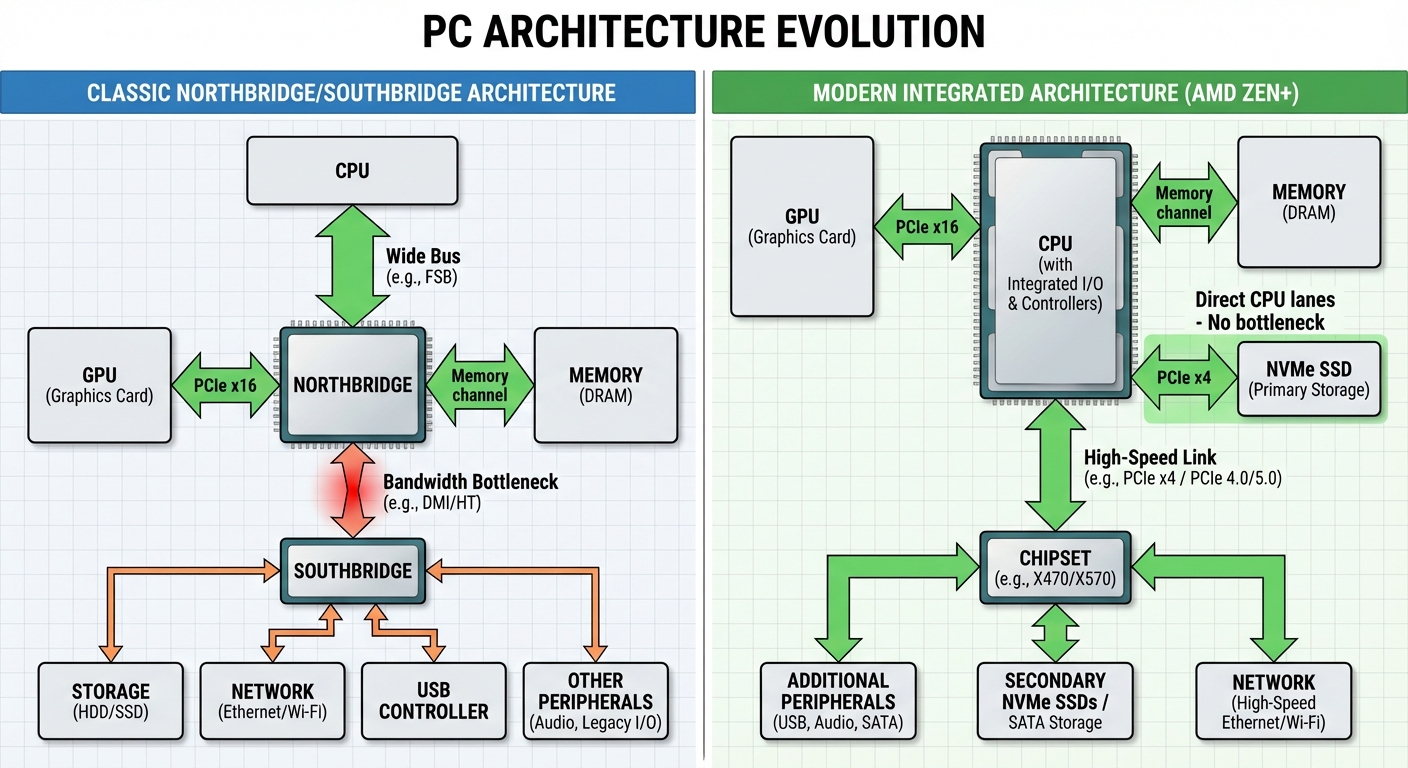
The Northbridge/Southbridge Era
From the late 1990s through the early 2010s, PC architecture followed a two-chip design:
- Northbridge: Handled high-speed components (CPU, GPU, memory)
- Southbridge: Handled everything else (storage, network, USB, audio)
All storage and network traffic had to funnel through the connection between Southbridge and Northbridge—typically DMI 2.0, providing around 2 GB/s of bandwidth. When hard drives peaked at 100-200 MB/s and gigabit ethernet at 125 MB/s, this was adequate.
The Bandwidth Explosion
NVMe SSDs changed everything. First-generation NVMe drives (2013-2014) delivered 2-3 GB/s sequential reads—enough to saturate the entire chipset connection. By 2020, flagship drives reached 7+ GB/s. The Southbridge connection had become a severe bottleneck.
AMD’s Zen Innovation
When AMD designed their Zen architecture (2017’s Ryzen 1000 series), they provided 4 dedicated PCIe 3.0 lanes directly from the CPU for an NVMe SSD. This gave the primary storage device ~4 GB/s of dedicated bandwidth, bypassing the chipset entirely.
With Zen 2 (Ryzen 3000, 2019), AMD moved to a chiplet design with a separate I/O die managing all PCIe and memory controllers. This architecture allowed for aggressive PCIe generation adoption:
- Ryzen 3000: PCIe 4.0 (doubled lane bandwidth to ~2 GB/s per lane)
- Ryzen 5000: Refined PCIe 4.0 implementation
- Ryzen 7000: PCIe 5.0, providing 24 lanes from the CPU:
- 16 lanes for GPU(s)
- 4 lanes for primary NVMe (~8 GB/s at PCIe 5.0)
- 4 lanes for chipset connection
Each PCIe generation doubles per-lane bandwidth: PCIe 3.0 provides ~1 GB/s per lane, 4.0 provides ~2 GB/s, and 5.0 provides ~4 GB/s. A PCIe 4.0 x4 NVMe drive can theoretically hit 8 GB/s—far exceeding older chipset connections.
Intel’s Response
Intel CPUs have provided direct PCIe lanes since Skylake (6th gen, 2015), but traditionally all 16 lanes were allocated to the GPU. With Rocket Lake (11th gen, 2021) and Z590 chipsets, Intel introduced lane bifurcation: the 16 CPU lanes could be split into x8+x4+x4 configurations, allowing direct CPU attachment for an M.2 drive while maintaining GPU connectivity.
Intel adopted PCIe 4.0 with 11th gen and PCIe 5.0 with 12th gen (Alder Lake), bringing their platforms to parity with AMD on bandwidth capabilities.
Why This Matters Now
The shift from chipset-routed I/O to CPU-direct connections explains modern bandwidth contention. Those CPU-attached PCIe lanes are a finite resource. When you install a second GPU, you’re often splitting the 16 GPU lanes into x8+x8. Add a direct-connected NVMe drive, and you might be pulling from the same pool. Add a high-speed network card or capture device, and the competition intensifies.
Understanding where your devices connect—CPU-direct lanes versus chipset lanes — is first step for diagnosing bandwidth starvation.
The Bandwidth Battle: When Your Second GPU Shares the Road
Every device connected to the chipset—your second GPU, NVMe drives, USB controllers, Ethernet, SATA ports—shares a single uplink back to the CPU.
Intel’s chipset uplink utilizes DMI 4.0, providing a bandwidth of approximately 15.75 GB/s unidirectional (and about 31.5 GB/s bidirectional) via PCIe 4.0 x8. In contrast, AMD limits its chipset uplink to PCIe 4.0 x4 (7.88 GB/s) but compensates by providing additional dedicated NVMe lanes (x4) that connect directly to the CPU, bypassing the chipset entirely. In this architecture, if a second GPU were to interface through the chipset, it would have to compete for bandwidth with all other active devices connected to that chipset.
When your second GPU routes through the chipset, it competes for bandwidth with every active device.
Why AI Training Hits This Hard
Gaming involves bursty PCIe traffic—the GPU loads scene data, renders frames internally, then sends finished frames back. AI training maintains sustained high-bandwidth transfers: datasets stream from storage to RAM, batches move to GPU memory, and gradients/checkpoints flow back for saving.
If both the secondary GPU and the NVMe drive are routed through the chipset, a “worst-case scenario” unfolds as the data path intersects with the aforementioned ‘Memory U-turn.’
Path: Device → Chipset → DMI → CPU → RAM → CPU → DMI → Chipset → Device
GPU Lanes vs. Chipset Bandwidth
The second GPU’s x4 PCIe 4.0 connection provides ~4 GB/s per direction simultaneously (full-duplex), totaling 8 GB/s aggregate bandwidth. Which bottleneck hits first depends on your workload and platform.
Upload Path (CPU → GPU):
- Training Data: RAM → Chipset → GPU
- NVMe Read: Storage → Chipset → RAM
- On AMD platforms like X570/B550 (4 GB/s chipset uplink), the chipset uplink often saturates before the GPU’s x4 lanes are fully utilized when disk reads and GPU data delivery occur simultaneously.
- On Intel DMI 4.0 (16 GB/s), the GPU’s x4 lanes are more likely to reach their limit first, provided the data loading load is moderate.
Download Path (GPU → CPU):
- Gradients/Checkpoints: GPU → Chipset → RAM
- NVMe Write: RAM → Chipset → Storage (during checkpoint saving)
- While saturating modern chipset links is less likely, latency increases due to contention still occur.
If you’re streaming large datasets from multiple NVMe drives while the GPU processes data, the chipset uplink becomes the bottleneck, especially on X570/B550 platforms. If training is primarily GPU-bound with moderate I/O, the GPU’s x4 lanes limit throughput first.
Direct SSD Lanes: A Partial Solution
Connecting your primary NVMe drive directly to CPU lanes (via the first M.2 slot on most boards) removes storage from chipset contention. Your disk traffic no longer competes with the second GPU for uplink bandwidth.
While this improves data loading performance, the second GPU still shares the chipset uplink with all other devices (Ethernet, USB storage, additional NVMe drives, SATA SSDs, or HDDs). If you perform distributed training that synchronizes gradients over the network or use multiple drives simultaneously, contention will persist.
The second GPU still operates on x4 PCIe lanes through a shared hub instead of direct CPU access. Whether the second GPU routes through the chipset depends on your motherboard’s PCIe lane distribution.
Motherboard Matters: The Lane Allocation
Understanding CPU PCIe lanes is key. Intel 12th–14th Gen desktop CPUs (12900K, 13900K, 14900K, etc.) provide 16 PCIe lanes directly from the CPU, typically configured as x16 for a single GPU or x8/x8 for dual GPUs. Additionally, they feature 4 dedicated PCIe 4.0 lanes for M.2 storage and a DMI 4.0 x8 link (~15.75 GB/s) for chipset connectivity. AMD Ryzen 7000 series provides a total of 24 usable PCIe 5.0 lanes (16 for GPU, 4 for NVMe, and 4 for additional NVMe) along with 4 PCIe 4.0 lanes for the uplink.
The chipset adds more lanes, but all chipset-connected devices share bandwidth through that single link to the CPU. Direct CPU lanes provide dedicated bandwidth; chipset lanes share a common pipe.
Key bandwidth figures (per direction):
- PCIe 3.0 x8: ~7.88 GB/s
- PCIe 4.0 x8: ~15.75 GB/s
- PCIe 5.0 x8: ~31.5 GB/s
PCIe 3.0 x16 provides the same bandwidth as PCIe 4.0 x8 (~15.75 GB/s), so generation matters as much as lane count.
Intel Z790 vs B760: Lane Splitting Differences
Intel motherboards handle multi-GPU differently based on chipset tier and board implementation:
Z790 (High-end): Typically supports PCIe bifurcation—the CPU’s 16 GPU lanes split into x8/x8, giving both GPUs direct CPU connection with 8 lanes each. Bifurcation requires both CPU support and board firmware support.
B760 (Budget): Bifurcation support varies by manufacturer despite being budget tier—check your specific board’s specifications. Boards without bifurcation typically route the first slot to all 16 CPU lanes and the second slot to x4 chipset lanes.
Note: Some boards drop from PCIe Gen 4 to Gen 3 when bifurcation is enabled. Verify this in your manual before assuming full Gen 4 speeds in x8/x8 mode.
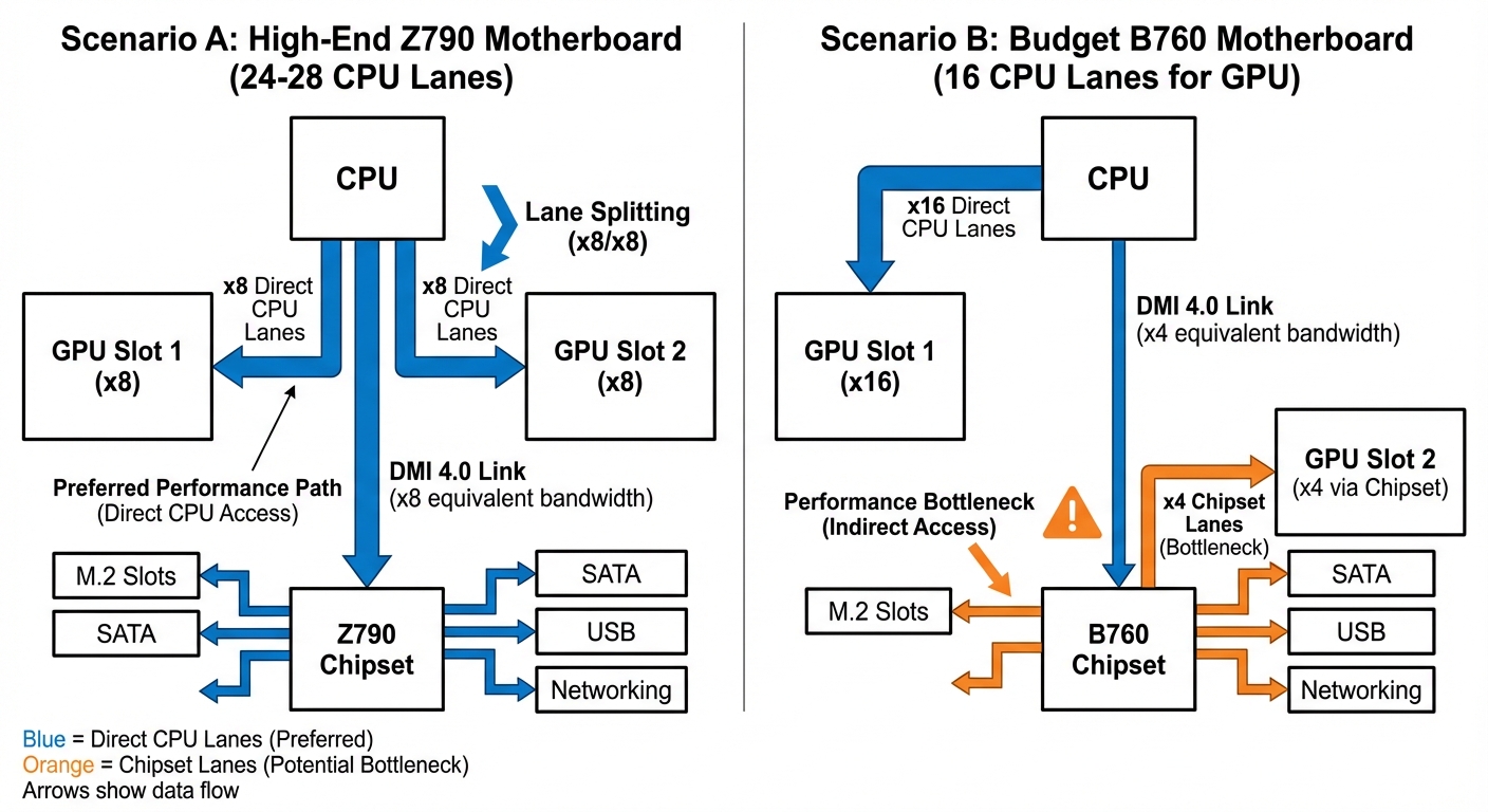
Scenario A: Proper Lane Splitting (Z790 with Bifurcation)
On a Z790 board with bifurcation enabled:
- GPU 1: PCIe 4.0 x8 direct CPU lanes (~15.75 GB/s per direction)
- GPU 2: PCIe 4.0 x8 direct CPU lanes (~15.75 GB/s per direction)
- M.2 slots use the 4 dedicated CPU lanes or chipset lanes
For multi-GPU AI workloads where both GPUs process different batches in parallel, x8 provides sufficient bandwidth. Bottlenecks appear when GPUs need frequent synchronization or large model transfers between devices—scenarios uncommon in typical inference or training setups where each GPU works on independent data.
Scenario B: The Chipset Bottleneck (B760 Without Bifurcation)
On boards without bifurcation support:
- GPU 1: PCIe 4.0 x16 direct CPU lanes (~31.5 GB/s per direction)
- GPU 2: PCIe x4 through chipset (shared bandwidth)
The chipset connection to the CPU (DMI 4.0 x8) provides ~15.75 GB/s total bandwidth shared across ALL chipset devices—SATA drives, USB controllers, network adapters, additional M.2 slots, and your second GPU. Your second GPU gets a fraction depending on concurrent activity, potentially as low as 2-4 GB/s under heavy I/O load.
AMD Chipset Comparison
AMD’s Ryzen 7000 platform follows similar patterns:
X670E/X670: Typically support bifurcation, allowing x8/x8 GPU configuration with PCIe 5.0 speeds. X670E provides more PCIe 5.0 lanes from the chipset.
B650E/B650: Bifurcation support varies by board manufacturer. B650E boards offer some PCIe 5.0 lanes; standard B650 typically uses PCIe 4.0 for GPU and storage.
The same chipset bandwidth sharing principles apply—direct CPU lanes beat chipset-routed lanes.
Lane Reallocation Options
Some motherboards allow trading M.2 slots for GPU connectivity. Disabling specific M.2 slots in BIOS can reallocate those CPU lanes to the second PCIe slot—potentially upgrading it from x4 chipset lanes to x4 direct CPU lanes. Your motherboard manual’s PCIe configuration matrix documents which slots share lanes and available reallocation options. Look for BIOS settings labeled “PCIe Slot Configuration,” “M.2/PCIe Sharing,” or “Bifurcation Mode.” Budget boards often hard-wire the configuration with no user control.
Asymmetric GPU Setups
For asymmetric configurations (e.g., RTX 4090 + RTX 3060), allocate all x16 lanes to the stronger GPU. Performance loss on the weaker card matters less for secondary tasks like inference on small models or video encoding.
Verify Your Current Configuration
Check your motherboard manual for the PCIe configuration matrix and block diagrams showing CPU vs chipset routing. Look for notes like “Slot 2 operates at x4 and shares bandwidth with M.2_3.”
To verify your running system’s actual configuration, use GPU-Z or HWiNFO—check both link width (x8/x16) and PCIe generation (3.0/4.0/5.0). BIOS settings don’t always reflect what’s actually negotiated.
Lane allocation determines theoretical maximum bandwidth to each GPU. The difference between x8 direct CPU lanes and x4 shared chipset lanes is measurable in multi-GPU AI work—but how much does it matter for your specific workload?
Deep Dive: Why Your Second GPU Trains Slower
Lane Inequality: The 4x Bandwidth Gap
PCIe lanes directly determine maximum throughput. The difference between configurations is significant:
- x16 lanes: ~32 GB/s per direction on PCIe 4.0 (64 GB/s aggregate)
- x8 lanes: ~16 GB/s per direction (32 GB/s aggregate)
- x4 lanes: ~8 GB/s per direction (16 GB/s aggregate)
A GPU running at x4 has 4x less bandwidth than one at x16. For CPUs with 24 lanes split between two GPUs, you might get x16/x4 or x8/x8 depending on bifurcation support. But chipset-connected GPUs typically get x4, and they face an additional problem.
Note that PCIe 3.0 delivers roughly half these numbers, while PCIe 5.0 doubles them. The generation matters as much as lane count.
The Training Data Pipeline
Training iterations follow this hot path:
Storage → RAM → GPU memory → Forward/Backward pass → Gradient sync
Each iteration requires:
- Loading the next batch from RAM to GPU memory
- Forward and backward pass computation
- Gradient synchronization (if using multiple GPUs)
Checkpoints save periodically to storage, not every iteration. But the sustained throughput demand during batch loading is where chipset GPUs struggle.
The Chipset Double Penalty
Chipset-connected GPUs face a compounding problem:
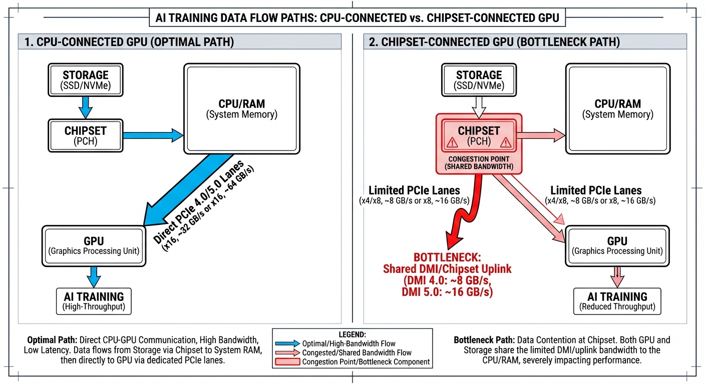
Storage reads and GPU data transfers both traverse the same chipset uplink to the CPU. With DMI 4.0’s ~8 GB/s per direction, your NVMe reads compete with GPU transfers for the same bandwidth when they occur sequentially in the data loading phase.
If your NVMe drives are also on the chipset (common in desktop builds), you’re sharing that ~8 GB/s uplink for:
- All storage read/write operations
- All GPU data transfers
- Any other chipset I/O (USB, SATA, network in some cases)
A CPU-connected GPU avoids this—its data comes directly from RAM via dedicated CPU lanes. Only the storage read competes for chipset bandwidth.
Prefetching mitigates this: Modern frameworks like PyTorch use multi-process data loaders that prefetch batches into RAM during GPU compute. With sufficient prefetch workers and fast RAM, the GPU can overlap computation with the next batch transfer. This is why chipset GPUs often perform better than raw bandwidth math suggests—the I/O happens while the GPU is busy computing.
Why Inference Doesn’t Care
Inference uses minimal I/O: models load once, inputs are small (kilobytes to megabytes vs gigabyte training batches), and there’s no backward pass. Bandwidth rarely matters when compute dominates. A 1 MB inference input at even 8 GB/s transfers in 0.125 ms—imperceptible compared to inference compute time.
When Bandwidth Actually Matters
Not all training jobs bottleneck on I/O. Whether your second GPU suffers depends on:
High I/O scenarios (where chipset connection hurts):
- Large vision models with high-resolution images (ImageNet, COCO datasets)
- Video processing where frames load continuously
- Datasets that don’t fit in RAM, requiring constant streaming from storage
- Frequent checkpointing to storage during training
- Insufficient data loader prefetch workers or slow RAM
Low I/O scenarios (where chipset connection is fine):
- Small datasets that fit entirely in RAM after first load
- Models with high compute-to-data ratios (large transformers on modest batch sizes)
- Training with cached preprocessed features
- Mixed precision training that reduces data movement
- Well-tuned data loaders with aggressive prefetching
If your dataset loads into RAM once and stays there, the chipset connection barely matters. GPU-to-GPU communication (if doing distributed training) and compute become the bottlenecks instead.
Should you optimize for equal lane distribution, or is an asymmetric setup acceptable for your workload?
The Balancing Act: When Equal Isn’t Optimal
Splitting PCIe lanes x8/x8 between two GPUs reduces each GPU’s bandwidth. This matters when your workload consistently saturates PCIe utilization above 70-80% during execution—brief spikes are usually fine.
When Concentration Beats Distribution
A deep learning training job that saturates PCIe bandwidth during data loading becomes bandwidth-constrained when you split lanes:
- Two x8 GPUs (PCIe 3.0): Each gets ~7.88 GB/s per direction, both training slower than optimal
- One x16 GPU (PCIe 3.0): Gets ~15.75 GB/s per direction, trains at maximum throughput
- Two x8 GPUs (PCIe 4.0): Each gets ~15.75 GB/s per direction—often sufficient
PCIe generation matters. An x8 Gen4 link provides the same bandwidth as x16 Gen3, so the x8/x8 split becomes much less problematic on newer platforms.
For a single training job that doesn’t parallelize across GPUs, one GPU at x16 may complete it faster than running the same job on one of two x8 GPUs. If bandwidth constraints limit each GPU to 60% of optimal speed, two GPUs provide 1.2x throughput versus one x16 GPU—better than one GPU alone, but you paid for two GPUs and didn’t get 2x throughput. Whether this matters depends on whether you have parallel workloads to fill both cards.
The Big & Small Strategy
For mixed workloads, consider an asymmetric configuration:
Big GPU (Slot 1, x16): High-performance card for training or compute-intensive tasks Small GPU (Slot 2, x8 or x4): Lower-end card (like a GTX 1650 or similar) for display output, video encoding, or light inference
Your primary workload runs at full bandwidth while the secondary GPU handles desktop compositing, Jupyter notebooks, or driving multiple monitors. While modern GPUs handle desktop compositing easily, dedicating a separate card avoids VRAM fragmentation and ensures your big GPU’s full memory is available for training.
Critical limitation: Many consumer boards drop slot 1 to x8 when populating slot 2, though higher-end chipsets (X570, Z690+) often support x16 + x4. For x16 + x8 simultaneously, you typically need HEDT platforms (Threadripper, Xeon W). Verify your specific board’s PCIe topology in the manual.
When to Split, When Not to
Before deciding on lane distribution:
When x8/x8 makes sense:
- Models that fit entirely in VRAM with minimal host transfers
- Inference serving where GPU compute is the bottleneck, not data loading
- Pure compute workloads with infrequent synchronization
- PCIe 4.0 or 5.0 systems where x8 provides ample bandwidth
When x16 (or x16 + x4) makes sense:
- Training large models with frequent host-device transfers
- High-resolution image processing requiring data streaming from system RAM
- Workloads with non-pinned memory transfers (check PyTorch DataLoader
pin_memorysetting—unpinned transfers are significantly slower) - PCIe 3.0 systems with bandwidth-sensitive workloads
Measure actual PCIe utilization during your typical workload using nvidia-smi dmon -s pcie or profiling tools like Nsight Systems. Check link throughput numbers before assuming you’re bandwidth-limited.
Diagnosing Your Bottlenecks: Tools and Techniques
Before optimizing for I/O bottlenecks, confirm they’re actually your problem.
GPU Topology
Check your hardware layout:
nvidia-smi topo -m # Show GPU topology and connection types
Connection types you’ll see:
NVLink: Direct GPU-to-GPU interconnect (ideal)PHB: Same PCIe host bridge (good)PIX: PCIe switch connection (acceptable)SYS: Cross-CPU socket communication (slower)
If GPU 1 has SYS connections while GPU 0 has PHB, you have asymmetric topology. The GPU closer to the CPU/PCIe root complex (typically GPU 0) gets lower-latency access to system memory and storage, while the second GPU traverses additional PCIe hops.
Monitor Real-Time PCIe Bandwidth
Watch PCIe traffic during training:
nvidia-smi dmon -s pucvmet # p=power, u=utilization, c=clocks, v=voltage, m=memory, e=encoder, t=temperature
Focus on the pcie_tx and pcie_rx columns showing PCIe throughput in MB/s.
Run this during training and watch for:
- PCIe rx bandwidth hitting ~12-14 GB/s on PCIe 3.0 x16 (theoretical max is 15.75 GB/s, but protocol overhead reduces usable bandwidth to ~80%)
- GPU utilization (sm) dropping to 60-80% when bandwidth saturates
- Asymmetric patterns: GPU 0 at 95% utilization while GPU 1 fluctuates between 50-90%
Compare Per-GPU Training Throughput
Measure samples/second on each GPU. In DDP training, use rank to identify GPUs:
import time
import torch.distributed as dist
from collections import defaultdict

throughput_stats = defaultdict(list)

for batch in dataloader:
    start = time.perf_counter()
    # ... training step ...
    elapsed = time.perf_counter() - start

    samples_per_sec = batch_size / elapsed
    gpu_id = dist.get_rank()  # In DDP, rank corresponds to GPU
    throughput_stats[gpu_id].append(samples_per_sec)
If GPU 1 consistently processes 20-30% fewer samples per second than GPU 0, you’ve found asymmetric data delivery.
Run P2P Bandwidth Tests
Measure actual GPU-to-GPU transfer speeds:
import torch

size = 1024 * 1024 * 1024  # 1GB
iters = 20
src, dst = 'cuda:0', 'cuda:1'

x = torch.empty(size, dtype=torch.uint8, device=src)
start, end = torch.cuda.Event(enable_timing=True), torch.cuda.Event(enable_timing=True)

# Warmup & Sync
for _ in range(5): x.to(dst)
torch.cuda.synchronize(src); torch.cuda.synchronize(dst)

# Benchmark
start.record()
for _ in range(iters): x.to(dst)
end.record()
torch.cuda.synchronize(dst)

# Result (GB/s)
avg_ms = start.elapsed_time(end) / iters
gbps = (size / (avg_ms / 1000)) / 1e9
print(f"P2P Bandwidth: {gbps:.2f} GB/s")
Expected bandwidth:
- *NVLink: 25-50 GB/s per link (GPUs like V100, A100)
- PCIe 3.0 x16: 12-14 GB/s unidirectional
- PCIe 4.0 x16: 24-28 GB/s unidirectional
If you’re getting significantly less, there’s congestion or misconfiguration.
Watch for Data Loading Phase Drops
GPU utilization plummeting during data loading indicates I/O starvation. Run nvidia-smi dmon and watch the sm (streaming multiprocessor) utilization:
# GPU 0: 98% -> 95% -> 97% -> 96%  (steady)
# GPU 1: 92% -> 65% -> 88% -> 58%  (drops during I/O)
GPU 1 is waiting for data while GPU 0 has priority access to the shared I/O path.
Red Flags Summary
You have an I/O bottleneck if (thresholds are approximate, vary by workload):
- PCIe bandwidth consistently saturates (>90% of theoretical max)
- GPU 1 utilization drops 15-30% below GPU 0 during training
- Per-GPU throughput shows 20%+ asymmetry
- P2P bandwidth tests show unexpectedly low cross-GPU speeds
nvidia-smi dmonshows correlated drops insmutilization when PCIerxsaturates
If you’ve confirmed bottlenecks and need maximum performance, there’s a more drastic solution.
When Desktop Isn’t Enough: The HEDT Solution
Desktop platforms bottleneck 3-4 GPU configurations. A Ryzen 9 7950X provides 24 PCIe 5.0 lanes from the CPU; Intel Core i9-13900K/14900K provide 20 lanes (16 PCIe 5.0 + 4 PCIe 4.0). Chipsets add lanes, but they connect through a shared uplink to the CPU—these aren’t direct CPU lanes with the same bandwidth characteristics. Beyond the bandwidth split, desktop motherboards often can’t physically accommodate 4 dual-slot GPUs, and the fourth slot typically shares lanes with M.2 or other peripherals.
PCIe 5.0 x8 provides the same bandwidth as PCIe 4.0 x16 (~32 GB/s bidirectional), so a 24-lane PCIe 5.0 CPU can theoretically run 3 GPUs at full PCIe 4.0 equivalent bandwidth. For 3-GPU configurations where the GPUs support PCIe 5.0, this works. But most workstation GPUs (A5000, A6000) and current-generation consumer cards still use PCIe 4.0, and you still hit physical slot limitations. Moving to 4 GPUs definitively requires more lanes.
High-End Desktop (HEDT) and server platforms provide dramatically more PCIe lanes directly from the CPU:
Direct CPU PCIe Lanes:
- Mainstream desktop (Ryzen 9 7950X): 24 lanes PCIe 5.0
- Mainstream desktop (Core i9-13900K): 20 lanes (16 Gen5 + 4 Gen4)
- Threadripper Pro 5000WX: 128 lanes PCIe 4.0
- EPYC 7003/9004: 128 lanes PCIe 4.0/5.0 (single socket)
- Xeon-W 3400: 64 lanes PCIe 5.0
With Threadripper Pro or EPYC, you get 4 GPUs at full x16 bandwidth (64 lanes), with 48+ lanes remaining for NVMe, networking, and expansion. HEDT platforms also support PCIe bifurcation across most slots, allowing flexible configurations that desktop boards rarely enable.
In this environment, the true synergy of performance optimization unfolds when Linux and NCCL are combined. NCCL goes beyond merely identifying that GPUs are plugged into the same CPU; it calculates the precise “inter-device distance” based on which Root Complex they are bound to within the CPU architecture. By scanning the system topology, NCCL identifies GPUs with the shortest physical distance and forcibly opens P2P DMA—a dedicated high-speed shortcut. In doing so, it completely bypasses the OS’s default “RAM U-turn” policy, ensuring that data travels directly between devices rather than wasting cycles in system memory.
Not all 128 lanes on EPYC/Threadripper Pro are available for PCIe slots. Platforms reserve lanes for chipset connectivity, BMC, and onboard devices. Expect 96-112 lanes available for expansion cards.
Why the Platform Investment Pays Off
A typical high-end GPU costs $1,600-2,000 (RTX 4090, A5000). Four of them: $6,400-8,000. A Threadripper Pro workstation costs $3,000-6,000 more than a comparable desktop build once you factor in the CPU ($1,500-5,000+), TRX50 motherboard ($800-1,200), and quad-channel ECC memory requirements.
If your workload saturates multiple GPUs simultaneously—data-parallel ML training, multi-GPU rendering, parallel simulation—investing in the platform to maximize GPU utilization makes the GPU array worth the cost. Stick with desktop platforms if you’re running one GPU-intensive task at a time or your workload doesn’t scale beyond 2 GPUs. HEDT is for scenarios where GPU utilization is the bottleneck, not CPU cores or memory.
HEDT platforms offer quad-channel (Threadripper Pro) or octo-channel (EPYC) memory bandwidth, which matters for workloads that move large datasets between system RAM and GPU memory.
For workloads requiring more than 4 GPUs or dedicated GPU-to-GPU interconnects beyond PCIe, datacenter technologies like NVLink and GPU-optimized server chassis become necessary.
Beyond Desktop: Datacenter Technologies
The bandwidth challenges we’ve discussed hit a wall at datacenter scale. Modern LLMs like GPT-4 or Llama 3 405B are too large to fit on a single GPU—they require distributed training across dozens or hundreds of GPUs, often spanning multiple servers. At this scale, PCIe and even standard networking become unacceptable bottlenecks.
The Multi-GPU Communication Problem
When training is distributed across GPUs, they need to constantly synchronize gradients and exchange model parameters. PCIe gives you ~32 GB/s theoretical bandwidth per direction (Gen4 x16), closer to 27-28 GB/s in practice. Even 100 GbE networking only delivers ~12.5 GB/s. For workloads that exchange hundreds of gigabytes per training iteration, these speeds don’t scale.
NVLink and NVSwitch: GPU-Native Interconnects
NVLink is NVIDIA’s high-bandwidth, direct GPU-to-GPU interconnect that bypasses the CPU entirely. The limitations of PCIe and DMA we have discussed so far are clear: no matter how hard Linux and NCCL try, they are ultimately trapped under the ceiling of the ‘PCIe’ protocol and ‘system memory bandwidth.’ NVLink was engineered by NVIDIA to shatter this ceiling, providing a dedicated interconnect that functions independently of the CPU and RAM.
- Overwhelming Bandwidth Gap: While the latest PCIe 5.0 x16 manages a mere 63 GB/s, NVIDIA’s H100 GPU achieves a total aggregate bandwidth of 900 GB/s via NVLink 4.0 (across 18 links). This is not only over 14 times faster than PCIe 5.0 but also nearly 10 times faster than the entire bandwidth of typical system memory.
- Complete Elimination of the ‘U-turn’: In an NVLink environment, data never even approaches the RAM. Once NCCL detects NVLink, it halts PCIe topology analysis and routes all data through these ultra-high-speed dedicated lines. This fundamentally blocks the ‘memory bandwidth contention’ issues previously discussed.
- Unified Memory Architecture: NVLink is more than just a fast pipe; it supports cache-coherent memory access between connected GPUs. This means if a GPU needs data located in a neighboring GPU’s VRAM, it can access it transparently as if it were its own memory (similar to a NUMA architecture). While slightly slower than local VRAM, this is incomparably faster than any detour through system memory.
This is point-to-point: GPUs don’t all connect to all other GPUs directly. Topology matters. NVLink enables cache-coherent memory access between connected GPUs, functioning like a NUMA architecture—faster than going through system memory, but with higher latency than local VRAM.
NVSwitch solves the topology limitation. It’s a physical switch fabric that enables all-to-all communication. A single NVSwitch chip has 18 ports with 8 NVLink connections each. In an NVIDIA DGX H100, four NVSwitches create a non-blocking fabric where all 8 GPUs can communicate with any other GPU at full NVLink speed simultaneously.
For context: AMD’s Infinity Fabric and Intel’s Xe Link offer similar concepts, but for NVIDIA GPUs, NVLink is the only option and has the ecosystem maturity. For training foundation models, these GPU-native interconnects are non-negotiable—the bandwidth requirements simply can’t be met any other way.
GPUDirect Storage: Eliminating the CPU Bottleneck
While NVLink solves GPU-to-GPU communication, there’s another bandwidth problem: getting training data from storage to GPUs.
Traditional path:
Storage → RAM → CPU (bounce buffer) → GPU
The CPU copies data from storage into system memory, then copies it again to GPU memory. This wastes memory bandwidth, burns CPU cycles, and adds latency.
GPUDirect Storage (GDS) eliminates the CPU from this path:
Storage → GPU (via DMA)
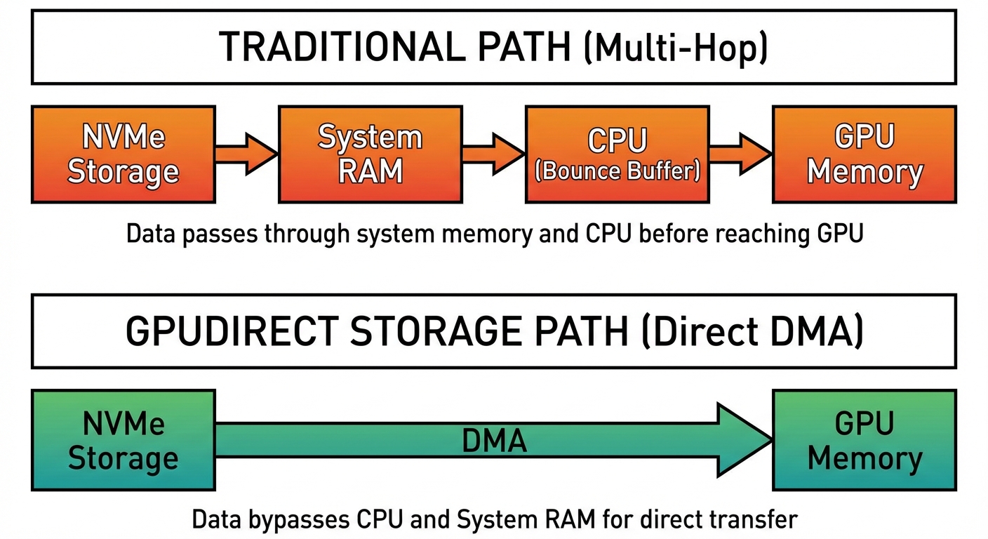
GDS requires PCIe peer-to-peer (P2P) support, allowing the NVMe controller to write directly to GPU BAR memory using DMA. Not all storage controllers or system BIOS configurations support this—it’s specific to datacenter-grade hardware.
Benefits:
- Higher bandwidth: No longer limited by CPU/memory throughput
- Lower latency: One transfer instead of two
- CPU freed up: Can focus on preprocessing, scheduling, or other training pipeline work
These datacenter technologies represent the other end of the bandwidth spectrum from desktop systems. While not practical for most use cases due to cost and infrastructure requirements, they show what’s possible when bandwidth becomes the absolute priority.
Conclusion: Matching Hardware to Workload
The x86 PCIe topology determines multi-GPU performance more than most spec sheets reveal. Your CPU dictates how many lanes are available, and your motherboard decides how to split them—usually in ways that prioritize single-GPU configurations.
Before you buy:
Check your motherboard’s manual for actual lane allocation. A board advertising “3x PCIe x16 slots” often runs them at x16/x0/x4 or x8/x8/x4 under load. Those numbers matter when you’re pushing 12GB/s per GPU.
Before you optimize:
Measure your actual bottleneck. Run nvidia-smi dmon -s pucvmet during training to see PCIe throughput. If you’re hitting 90%+ GPU utilization with x8 lanes, your bottleneck isn’t I/O—it’s elsewhere in your pipeline. Adding lanes won’t help.
Platform reality:
Desktop CPUs (Ryzen 5/7, Core i5/i7/i9) typically provide 20-24 usable PCIe lanes total. That’s enough for two GPUs at x8 plus NVMe storage. Need three or four high-bandwidth GPUs? That’s what Threadripper, Xeon W, and EPYC exist for—they offer 64-128 lanes but cost accordingly.
Economic optimization:
A $2000 HEDT platform makes sense when you need 4x A6000s running at x16. It doesn’t make sense for running Stable Diffusion twice as fast. Match your hardware investment to workload revenue or time savings. “Good enough” is often optimal when x8 gives you 95% of x16 performance.
The real question isn’t “can I run multiple GPUs”—it’s “does my workload justify the platform that supports them properly.” Armed with PCIe topology knowledge, you can answer that honestly and avoid both under-buying (x4 bottlenecks) and over-buying (unused lanes on a $3000 motherboard).
Check your lanes, measure your bottlenecks, buy what you’ll actually use.